

Artificial intelligence has a bandwidth crisis, and Ayar Labs sits at the center of a new approach to solving it. This article dives into its technology, products, and the competitive landscape shaping the future of AI infrastructure.
1. The Problem: AI’s Copper Ceiling
The core constraint in modern AI systems is not how fast chips can compute, but how efficiently they can move data. While GPU transistor counts continue to scale according to Moore’s Law, the copper interconnects linking chips, memory, and racks are reaching their physical limits. As AI clusters grow from hundreds to tens of thousands of accelerators, these connections consume significant power, generate heat, and introduce latency. NVIDIA estimates that a single AI rack using electrical I/O can draw nearly 600 kW, much of it spent moving data rather than processing it. In hyperscale environments, interconnect power can even exceed the compute budget, a constraint often referred to as the memory wall or bandwidth wall.
Semiconductor research shows that in modern AI systems, about 60 to 80 percent of energy is spent moving data between memory, processors, and chips. And in that 600 kW AI rack, only about 120-180 kW (20-30%) goes toward actual mathematical computation. The remaining 420-480 kW (70-80%) is burned shuttling data around through copper wiring.
Replacing copper with silicon photonics could fundamentally shift this ratio. Optical I/O reduces interconnect energy from 15-20 picojoules (pJ) per bit (copper) to approximately 5 pJ/bit today, with a roadmap to below 1 pJ/bit. This would push the power split from 20-30% computation toward 40-50%, and when combined with emerging in-memory computing approaches, potentially to 60-70% computation. The table below illustrates the shift:
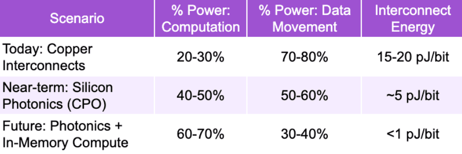
Sources: NVIDIA Technical Blog, SemiAnalysis, CMU Research, IEEE Spectrum, Ayar Labs
Copyright © Jarsy Research
2. Founding Story and Technical Origins
Addressing this constraint requires rethinking the interconnect itself. That is the premise behind Ayar Labs. Founded in 2015 in San Jose, Ayar Labs emerged from a decade-long collaboration between researchers at MIT, UC Berkeley, and the University of Colorado Boulder. The foundational work was supported by DARPA’s POEM program, which aimed to demonstrate that optical I/O could be built using standard silicon manufacturing processes.
The company was co-founded by Mark Wade, Chen Sun, Alex Wright-Gladstein, Vladimir Stojanovic, Rajeev Ram, and Milos Popovic. Wade, who initially served as Chief Scientist and CTO, became CEO in December 2023. The founding team brought together expertise in photonics, CMOS chip design, and systems architecture, a combination that is rarely found in a single company.
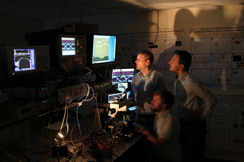
Founders of Ayar Labs. Image Credit: Ayar Labs
At the core of Ayar Labs’ approach is a practical insight. Silicon photonics, the ability to guide light through waveguides on a chip, can be manufactured using existing CMOS* foundry processes. This makes it possible to produce optical chiplets at scale in the same facilities that fabricate processors, without relying on specialized materials.
*CMOS (Complementary Metal-Oxide-Semiconductor) foundry is a semiconductor manufacturing facility that fabricates chips using the CMOS process, the dominant technology for making virtually all modern processors, memory chips, and integrated circuits.
3. Ayar Labs’ Optical I/O Platform: TeraPHY and SuperNova
Ayar Labs’ approach is not a single chip, but a system level optical I/O platform designed to replace the most power intensive electrical interconnects. Its co packaged optics solution centers on two components: an optical chiplet (TeraPHY) integrated next to the processor, and a shared external light source (SuperNova).
Together, they form a new data movement layer where information is transmitted as light directly from the chip package, bypassing much of the electrical path across boards and racks.
Instead of sending signals through copper, data is encoded onto light inside the package, transmitted through fiber, and converted back into electrical form at the destination. Moving this conversion point closer to the processor reduces both energy and latency.
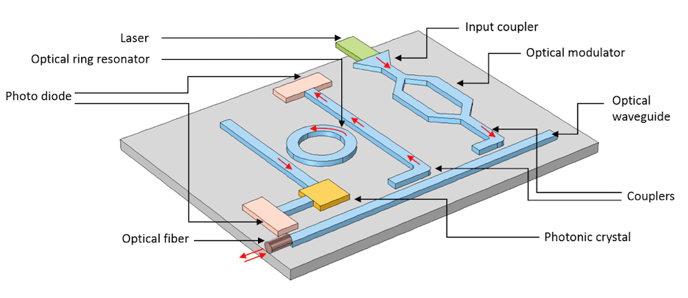
TeraPHY: Optical I/O Chiplet
TeraPHY is the compute side interface. It is a silicon photonics chiplet integrated alongside a GPU, CPU, or AI accelerator within the same package. Its function is to convert electrical signals into optical signals and back again, enabling high bandwidth communication directly from the chip.
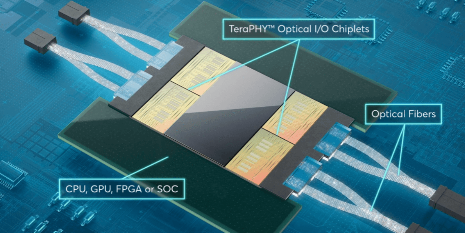
Image Credit: Semicone.com
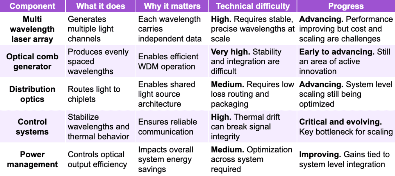
The main components of TeraPHY and their functions are as below:
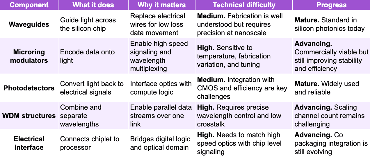
Sources: Mainly Ayar Labs, Copyright © Jarsy Research
Optical waveguides. Image Credit: Comsol.it
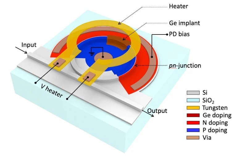
Microring modulators. Image Credit: https://www.researchgate.net/
SuperNova: External Laser Source
SuperNova provides the light used for data transmission. Instead of placing lasers on every chip, Ayar centralizes the light source into a shared external module that supplies many TeraPHY chiplets across the system.
SuperNova is the external light engine that powers Ayar Labs’ optical I/O system. It is a multi wavelength, multi port laser source that supplies up to 16 wavelengths across 16 fibers, enabling 256 data channels and up to 16 Tbps of total capacity. Instead of placing lasers on every chip, Ayar centralizes the light source into a shared module that feeds multiple TeraPHY chiplets. By separating the laser from the photonic chip, this design avoids the thermal challenges of on-chip lasers while enabling a more scalable and manufacturable architecture.
The main components of SuperNova and their functions are as below:
Sources: Ayar Labs, Other public information. Copyright © Jarsy Research
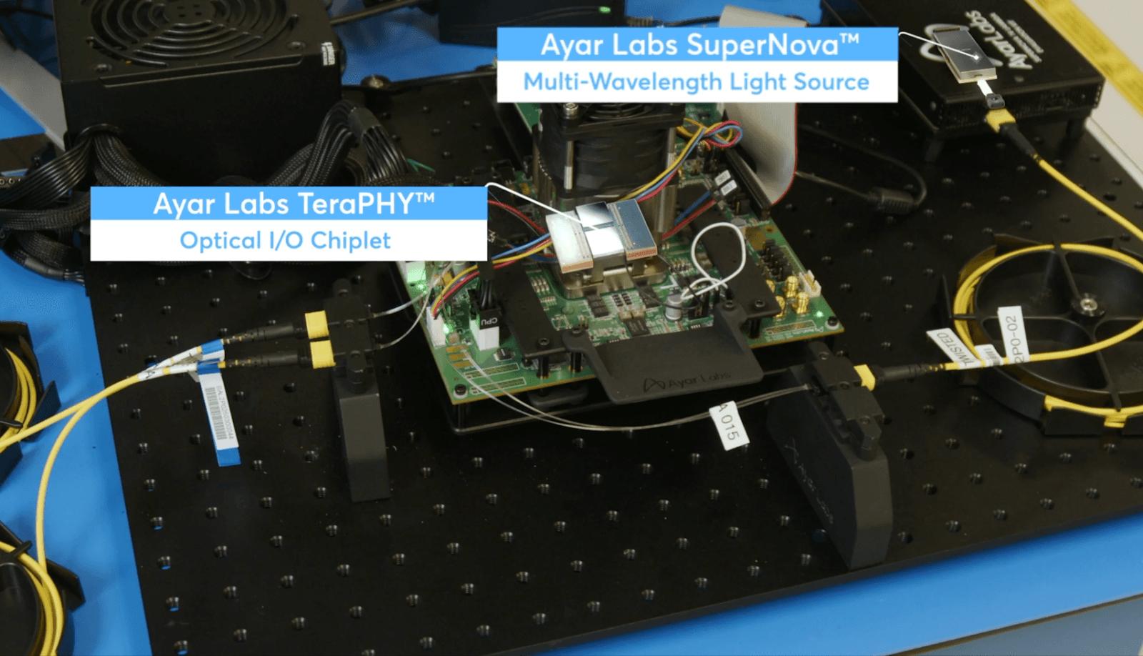
TeraPHY and SuperNova. Image Credits: Ayar Labs
Optical vs. Copper: Performance Comparison:
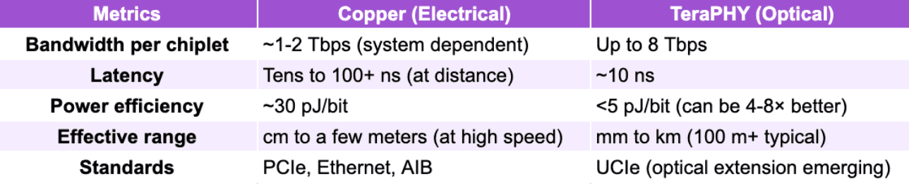
Sources: Ayar Labs, Other public information. Copyright © Jarsy Research
4. Funding rounds and Valuation
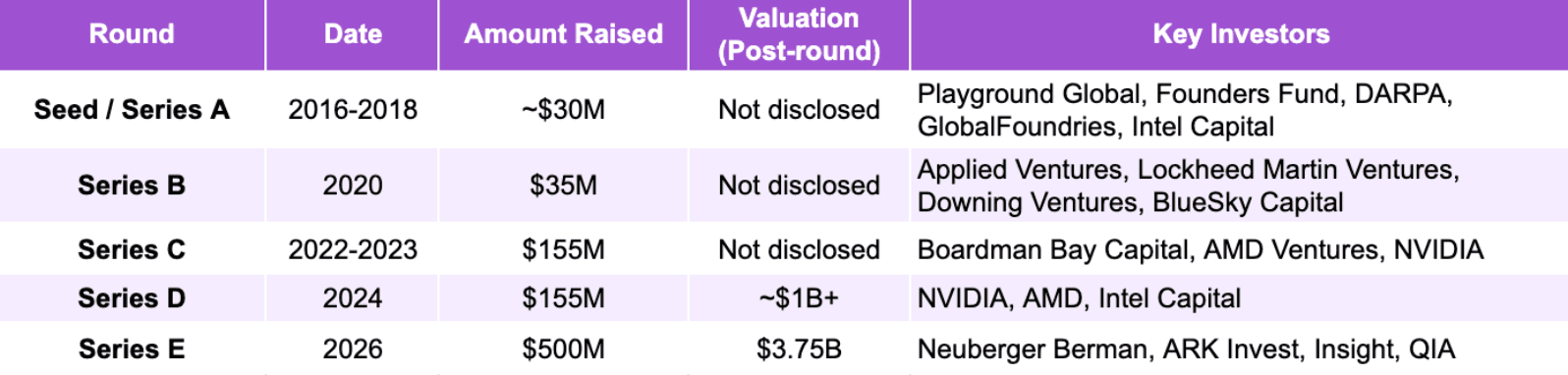
Ayar Labs has raised a total of approximately $870 million across five rounds of equity funding. Its most recent Series E, announced on March 3, 2026, raised $500 million and valued the company at $3.75 billion. The round was led by Neuberger Berman with participation from ARK Invest, Insight Partners, MediaTek, the Qatar Investment Authority, Sequoia Global Equities, Alchip Technologies, and 1789 Capital.
Sources: Crunchbase, Ayar Labs. Copyright © Jarsy Research
5. Competitive Landscape and Strategic Moat
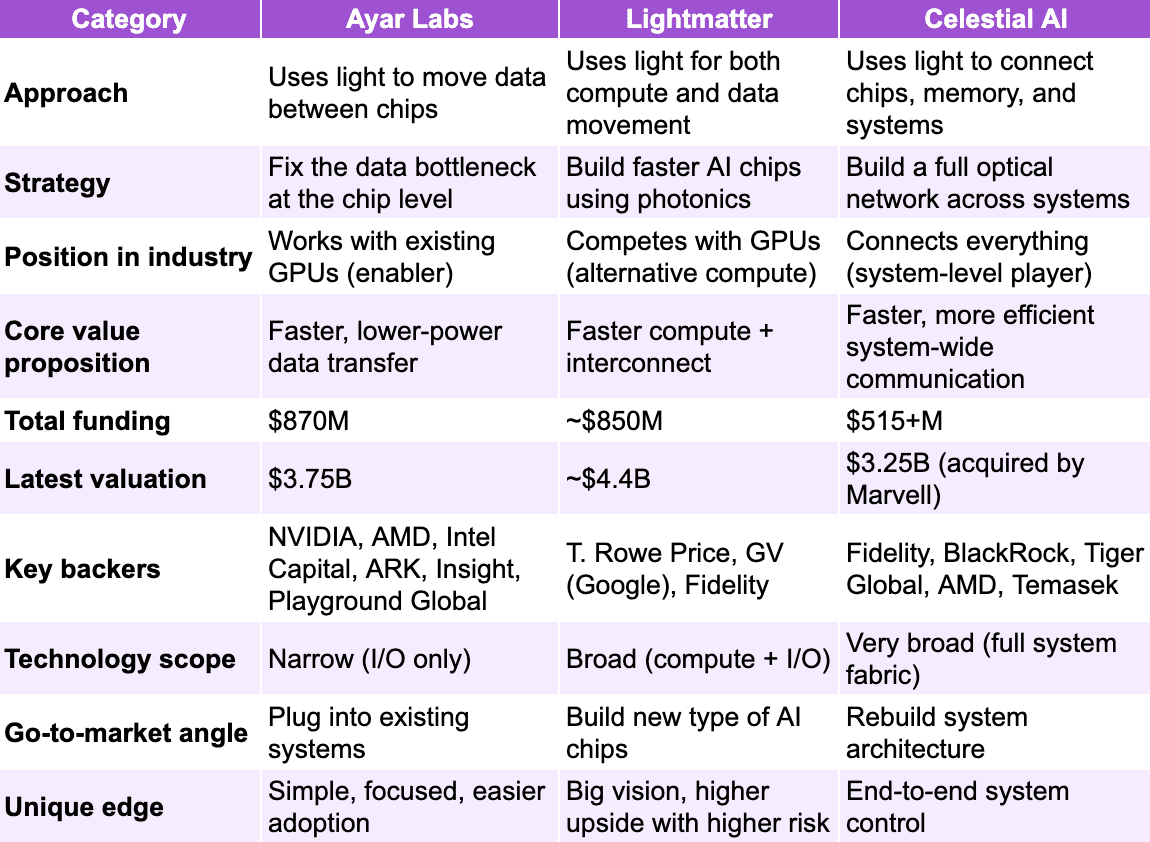
Ayar Labs operates in an increasingly crowded space, with several well-funded startups pursuing different approaches to photonic interconnects for AI data centers. Two stand out as primary competitors.
Lightmatter ($850M raised, $4.4B valuation) leads with its Passage 3D photonic interconnect platform, featuring wafer-scale programmable photonic switches, high-density DWDM transmission, and a software layer called Idiom. Lightmatter’s approach is more vertically integrated: it builds photonic compute (Envise), interconnect (Passage), and software in a single stack. Its edgeless I/O design covers the entire die area rather than the modular chiplet approach Ayar uses.
Celestial AI focuses on its Photonic Fabric technology, which decouples memory from compute to enable ultra-high bandwidth (14.4 Tbps) memory transactions. Celestial’s approach targets the memory wall specifically, aiming to create a new memory architecture rather than replacing chip-to-chip wiring.
Ayar’s strategic moat rests on three pillars. First, its technology is built on standard CMOS processes, meaning it can be manufactured at existing foundries without exotic materials or dedicated fabs. Second, Ayar has championed open standards (particularly UCIe), which positions it as the ecosystem-friendly option for hyperscalers who prefer interoperable solutions over proprietary lock-in. Third, the simultaneous backing of NVIDIA, AMD, and Intel gives Ayar a level of industry validation that no competitor has matched.
Sources: Crunchbase, Ayar Labs, Lightmatter, Sacra, Celestial AI, Reuters.
Copyright © Jarsy Research
6. Looking Ahead
The opportunity for Ayar Labs is expanding alongside the rapid growth of AI infrastructure. While the optical interconnect market alone is projected to reach ~$40B by 2030 and grow toward $60B-$70B by 2035, this represents only one layer of a much larger shift. As photonics moves deeper into chip design, packaging, and system architecture, the broader data movement stack could evolve into a market well beyond $100B.
The next 18 months will be critical. Ayar Labs must demonstrate it can scale manufacturing, secure design wins with major hyperscalers, and transition from promising technology to widespread deployment. If it succeeds, Ayar could become one of the defining infrastructure companies of the AI era - the company that brings light to silicon.⚡✨
Further reading: Ayar labs website, IEEE Spectrum: Optical Interposers for AI, Ayar Labs CEO Interview, Contrary Research on Ayar Labs


