
For decades, general-purpose processors dominated because flexibility mattered more than efficiency. AI is changing that balance. Its growing demand for capital, electricity and data-centre capacity is pushing Google, Amazon, Microsoft and Meta to develop custom accelerators, while startups such as Etched, MatX and d-Matrix build purpose-designed alternatives to GPUs. This report examines the technologies, economics and companies shaping the custom AI silicon market.
1. What an ASIC is, and what it is not
An application-specific integrated circuit, or ASIC, is a chip designed for a defined application rather than general-purpose computing. The application may be narrow, such as Bitcoin mining or video encoding, or broader, such as accelerating a family of AI models. By tailoring compute, memory and data movement to the workload, an ASIC can deliver more performance per watt, dollar and unit of silicon.
This efficiency requires substantial upfront investment in chip design, verification, manufacturing, packaging and software. These costs are justified only when the workload is valuable, scalable, stable and long-lived.
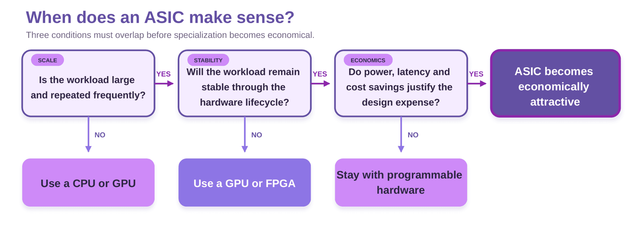
Figure 1: When does an ASIC make sense? © 2026 Jarsy Research
Unlike an FPGA (field-programmable gate array), a chip whose logic can be reprogrammed after manufacturing, an ASIC’s underlying circuits are fixed. Firmware and software may still change how an ASIC is used, and some ASICs contain programmable cores, but a flaw or major architectural change usually requires a new silicon revision, known as a respin.
An ASIC is not necessarily limited to one operation or to AI. Google’s TPU, smartphone image processors, networking chips and Bitcoin-mining processors are all ASICs. They may operate as standalone processors or as specialized components within larger systems.
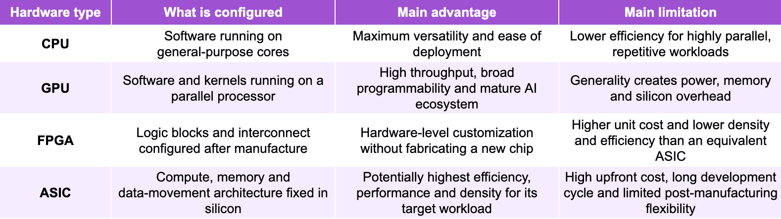
Table 1: Computing alternatives. © 2026 Jarsy Research
2. From Gate Arrays to AI Accelerators
Early custom chips were built using gate arrays: partially manufactured silicon customized through its final wiring layers. Ferranti commercialized this approach in products such as the ZX Spectrum, while LSI Logic later expanded access to custom-chip design and manufacturing.
During the 1990s, hardware-description languages, automated design tools and reusable IP blocks made custom silicon faster and less costly to develop. Designers could increasingly describe a chip’s functions in code, automate parts of the design process and reuse components such as CPU cores, memory controllers and high-speed interfaces.
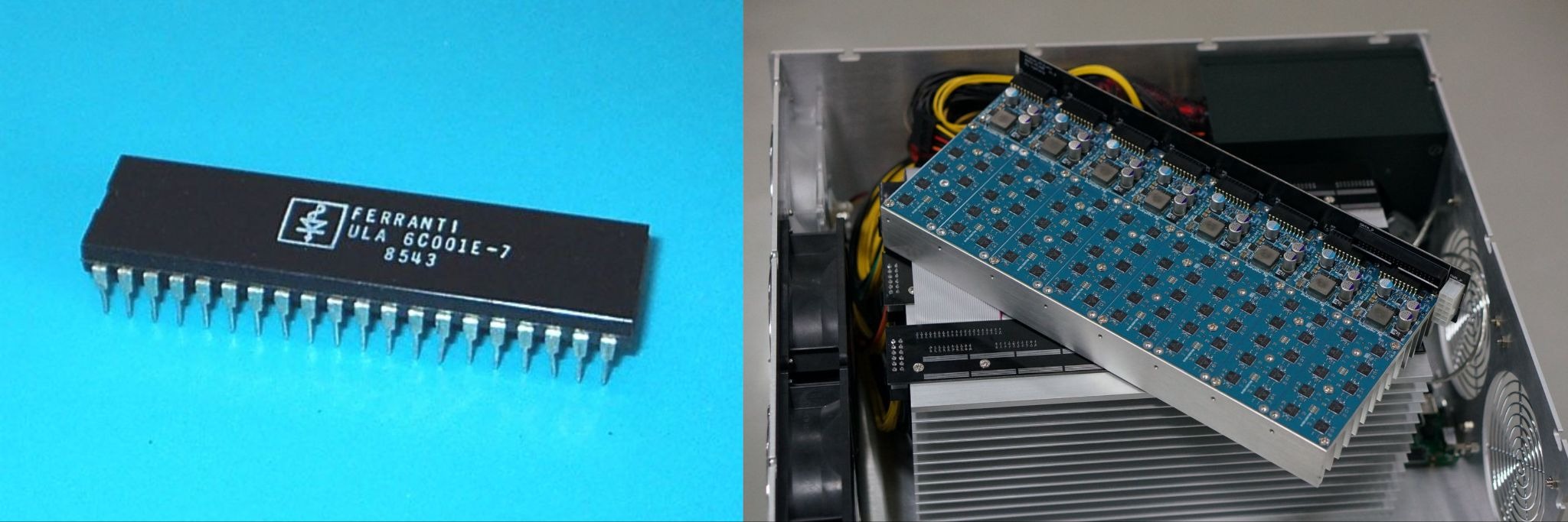
Ferranti’s ULA6C001E7, a gate-array chip used in the ZX Spectrum (left); The Avalon Bitcoin miner was among the earliest purpose-built ASIC mining systems. Image Credits: Wikipedia
Bitcoin mining later provided a clear demonstration of specialization. As the workload became large and predictable, mining progressed from CPUs to GPUs, FPGAs and finally ASICs, which proved far more efficient at repeatedly calculating the same hashing algorithm. Avalon shipped one of the first commercial Bitcoin ASIC mining systems in 2013.
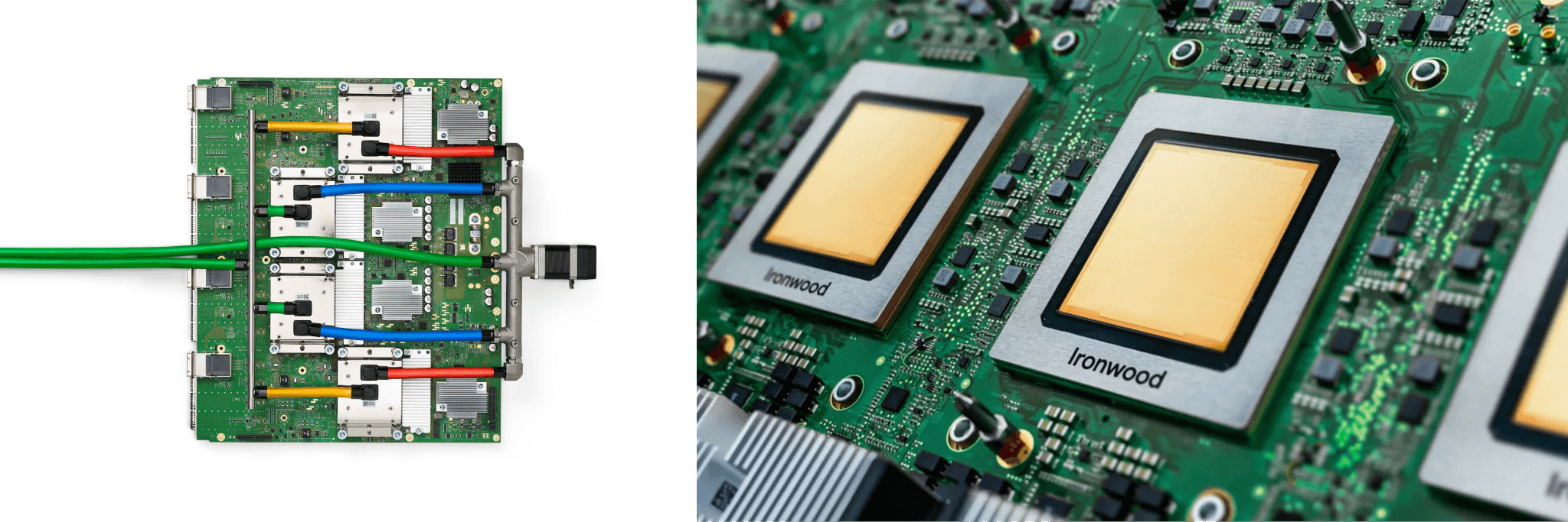
Google’s TPU v4 (left); Google TPU v7 Ironwood (right). Image Credits: Google
AI followed the same economic principle at a much greater scale. Google deployed its first TPU for neural-network inference in 2015 and later expanded the architecture into training, cloud services and large multi-chip systems. The TPU demonstrated how a stable, high-volume workload could justify an entire custom computing platform.
3. How AI Workloads Shape Chip Design
AI is not a single workload. Pre-training builds foundation models, while post-training adapts them. Inference includes prefill, which processes the input prompt, and decode, which generates the response one token at a time. Recommendation systems, multimodal models and edge applications create different demands again. A chip optimized for one workload may therefore be less effective for another.
3.1 Different workloads, different hardware
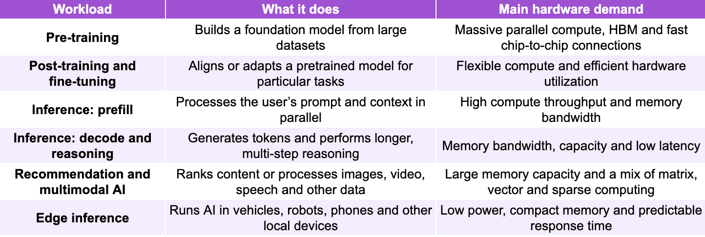
Table 2: Main AI Workloads and hardware demand. © 2026 Jarsy Research
Training and prefill can spread calculations across many processors. Decode is more sequential, generating one token at a time and often spending more time retrieving data than calculating. Agents and reasoning models amplify this challenge through longer outputs, repeated model calls and larger contexts. They depend on sustained inference speed, memory capacity and low latency, not just peak computing power.
3.2 How an AI ASIC Works
An AI ASIC improves efficiency by designing its compute units, memory and data movement around a defined family of workloads. The objective is not simply to perform more calculations, but to keep useful data close to the compute units and remove hardware features the workload does not need.
3.2.1 Specialized compute engines
Neural networks rely heavily on matrix multiplication. If matrix A has dimensions M×K and matrix B has dimensions K×N, calculating: C=A×B requires approximately:
Operations≈2MKN
AI ASICs perform these calculations through thousands of multiply-accumulate, or MAC, units:
y←y+(a×b)
Instead of using a small number of flexible CPU cores, thousands of MAC units perform these operations in parallel. Example: Multiplying two 4,096 × 4,096 matrices requires approximately:
2 × 4,0963 ≈ 137 billion operations
A processor capable of 1 petaflop (1015 operations per second) could theoretically complete about 7,300 such multiplications per second. Real performance is lower because compute units must wait for memory, communication and scheduling.
Google’s TPU, for example, uses a systolic array in which model weights and input data flow through a grid of MAC units. Each value is reused several times before leaving the array, reducing repeated memory access. Other ASICs use tensor engines, vector engines, dataflow processors or compute-in-memory arrays. The implementation differs, but the aim is the same: devote more of the chip to the calculations the target workload actually uses.
3.2.2 Memory and data movement
Moving data can consume more time and energy than performing the calculation itself. An AI ASIC must therefore decide what data remains on the chip, what is stored in external memory and how often it moves.
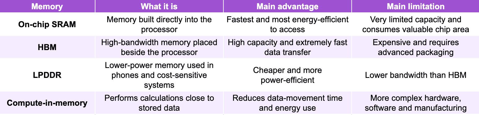
Table 3: Memory types. © 2026 Jarsy Research
Numerical precision also affects memory and performance. The approximate storage required by a model is:
Model size = Number of parameters × Bits per parameter / 8

Table 4: Model sizes for a 70-billion-parameter model. © 2026 Jarsy Research
Lower-precision formats such as FP8 and FP4 reduce memory requirements and can increase processing speed, but they may also affect model quality. The best format depends on the model, workload and hardware.
3.3 The architectural choices that matter
An AI ASIC is part of a larger computing system. Its performance depends on six connected choices: compute architecture, memory, data movement, numerical precision, programmability and software. Greater specialization can improve efficiency, while greater flexibility allows the chip to support a wider range of models and workloads.
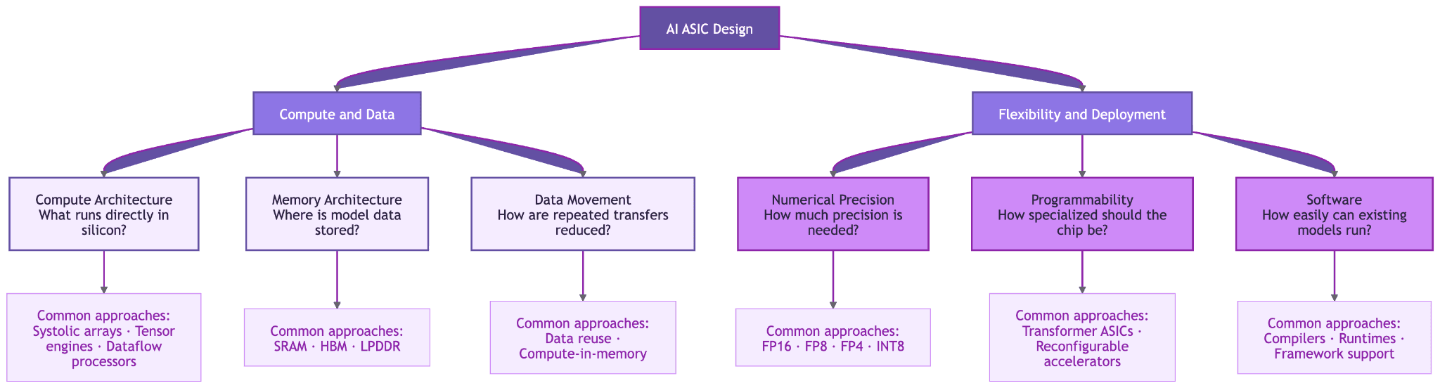
Figure 2: Design choices behind an AI ASIC. © 2026 Jarsy Research
4. Three Routes to Custom AI Silicon
Custom AI silicon reaches the market through three main routes. These are business models rather than strict technical categories, and some companies operate across more than one.
4.1 Three routes to market
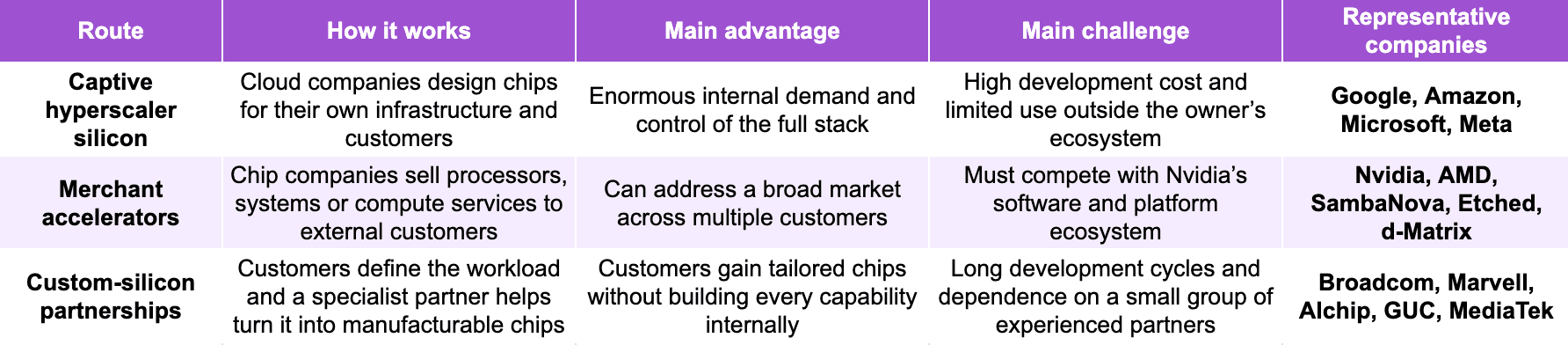
Table 5: Three Routes to Custom AI Silicon. © 2026 Jarsy Research
Examples: Google can optimize a TPU for its own models, software and data centres. A merchant supplier such as Etched must support external customers and prove that its advantage survives unfamiliar models and operating environments. Broadcom can participate in several customer programs without betting its entire business on one accelerator architecture.
4.2 The hyperscaler programs
Hyperscalers are the centre of the custom-silicon market because they have enough predictable demand to justify developing their own chips. These accelerators lower the cost of high-volume workloads, differentiate cloud services and reduce reliance on merchant GPUs.
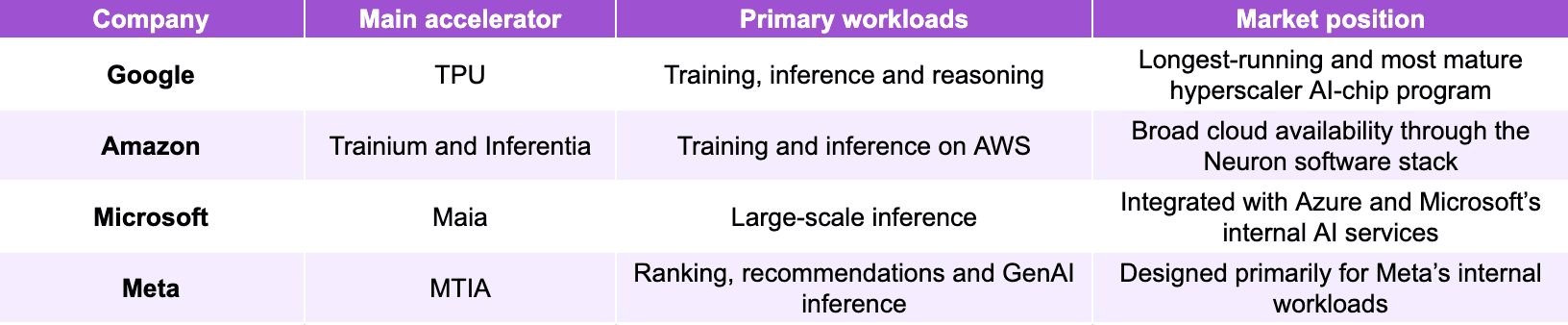
Table 6: Main Hyperscalers and their processors. © 2026 Jarsy Research
Huawei Ascend, Alibaba Hanguang and Baidu Kunlun represent important Chinese custom-AI programs, although their commercial models and public disclosures differ from those of the US hyperscalers.
Google TPU: the reference case
Google’s TPU is the clearest example of custom AI silicon developing into a complete computing platform. The first generation focused mainly on inference, while later generations expanded into training, cloud services and multi-chip systems.
Ironwood became generally available on March 31, 2026 and can scale to 9,216 chips per pod. Google’s eighth-generation TPU 8t and TPU 8i take specialization further: TPU 8t is optimized for large-scale training, while TPU 8i targets inference, reasoning and reinforcement learning. The two designs show that these workloads are now large and distinct enough to justify separate processors.
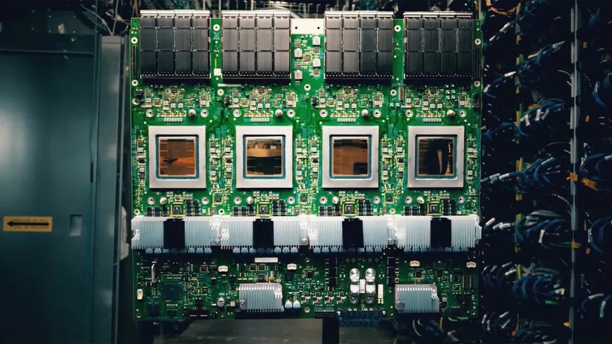
Ironwood. Image Credit: Google
4.3 Merchant accelerators
Merchant suppliers sell chips, systems or computing services to outside customers. This is where most AI-chip startups compete.
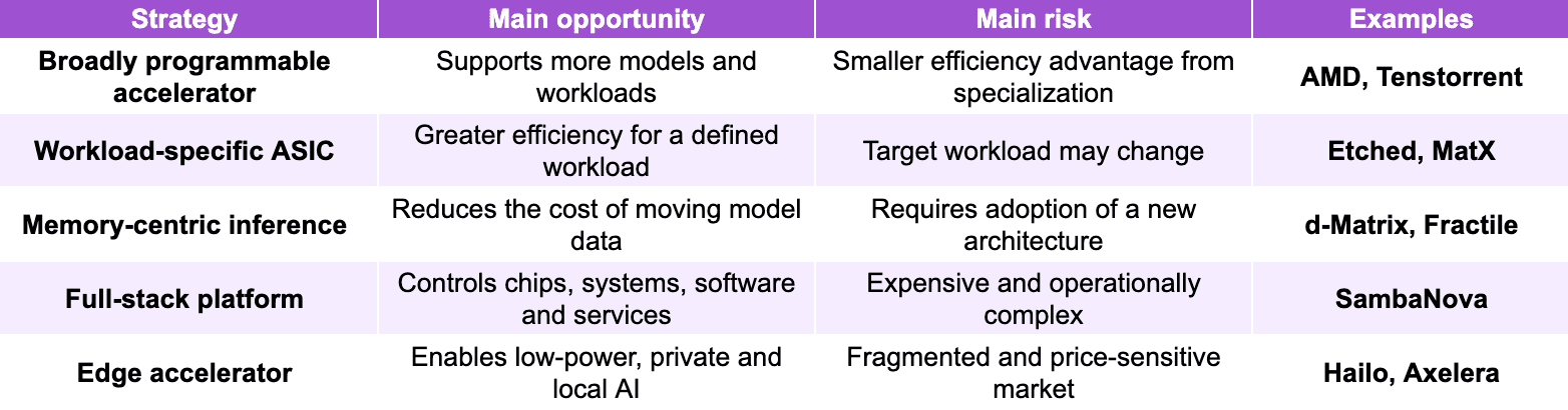
Table 7: Merchant accelerators. © 2026 Jarsy Research
Performance alone is insufficient. A merchant accelerator also needs reliable systems, software compatibility, customer support and production capacity. Chapter 5 examines the most important private challengers in greater detail.
4.4 Custom-silicon partners
Hyperscalers often design their chip architecture internally but rely on partners for implementation, networking and manufacturing. Broadcom and Marvell lead this market, while Alchip, GUC and MediaTek support selected custom-chip programs. Few startups compete here because hyperscalers favour experienced partners with proven IP, foundry relationships and the resources to manage long-term projects.
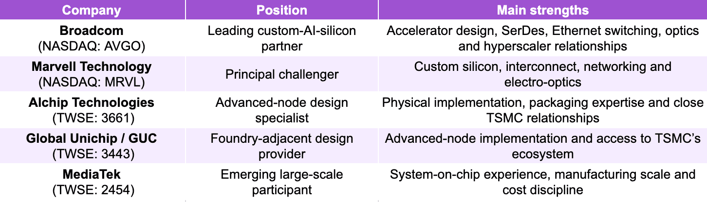
Table 8: Main custom-silicon partners. © 2026 Jarsy Research
5. The Start-up Map
AI-chip startups should not be placed in a single ranking: they target different workloads, customers and deployment environments. This chapter focuses on nine companies that combine differentiated technology, substantial financing or meaningful commercial validation.
5.1 Leading private AI-chip companies
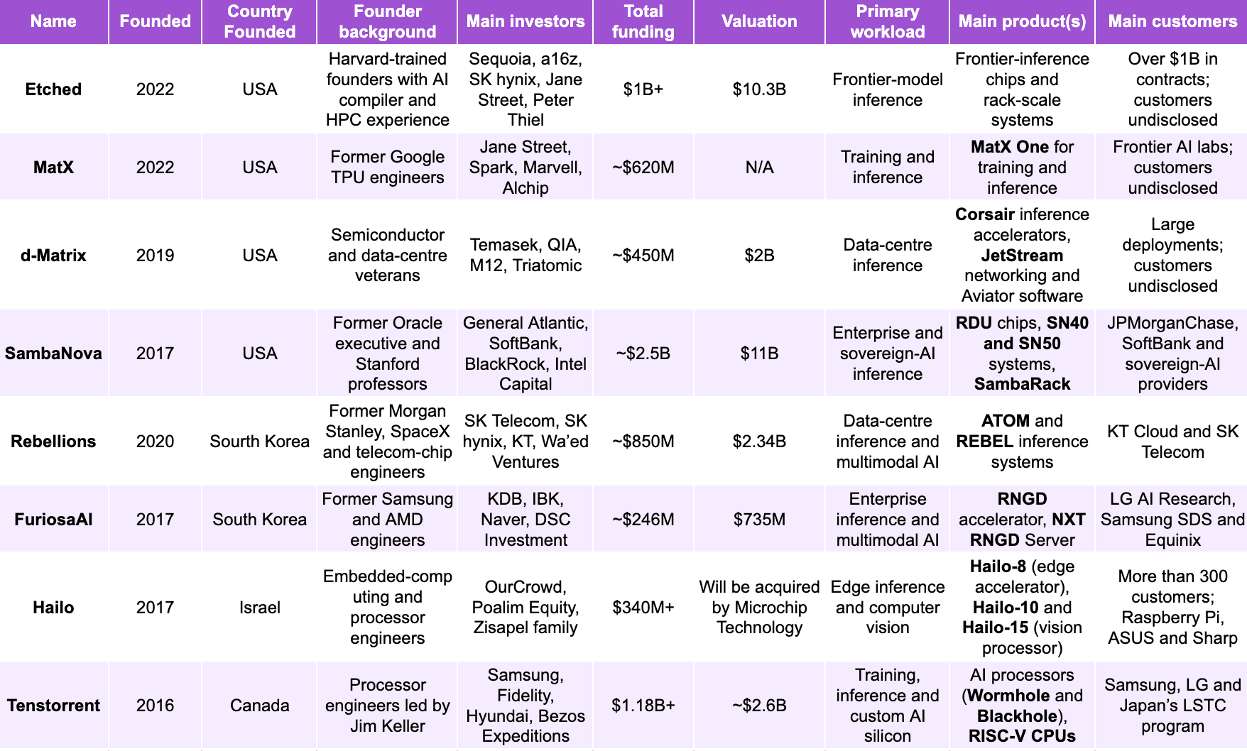
Table 9: Some of the leading AI-Chip start-ups. Data sources: Reuters, Crunchbase, Sacra, Yahoo Finance, CNBC, Forge Global, Microchip, tracxn. © 2026 Jarsy Research
5.2 Selected leaders across the private AI-chip companies
The following companies represent five important startup strategies: transformer specialization, memory-centric inference, dataflow systems, edge computing and licensable processor IP.
5.2.1 Etched: Frontier-model specialization (the highest-conviction architecture bet)
Etched was founded in 2022 by Harvard students Gavin Uberti, Chris Zhu and Robert Wachen, who believed transformers would become the dominant AI architecture. They left Harvard to build Sohu, an ASIC dedicated to transformer inference.
Etched now co-designs chips, memory, interconnect, software and rack-scale systems for both prefill and decode. It leads this category because its first silicon has returned from TSMC N4P and the company reports more than $1 billion in customer contracts. Its specialization could produce substantial efficiency gains, but also exposes it to changes in model architecture.
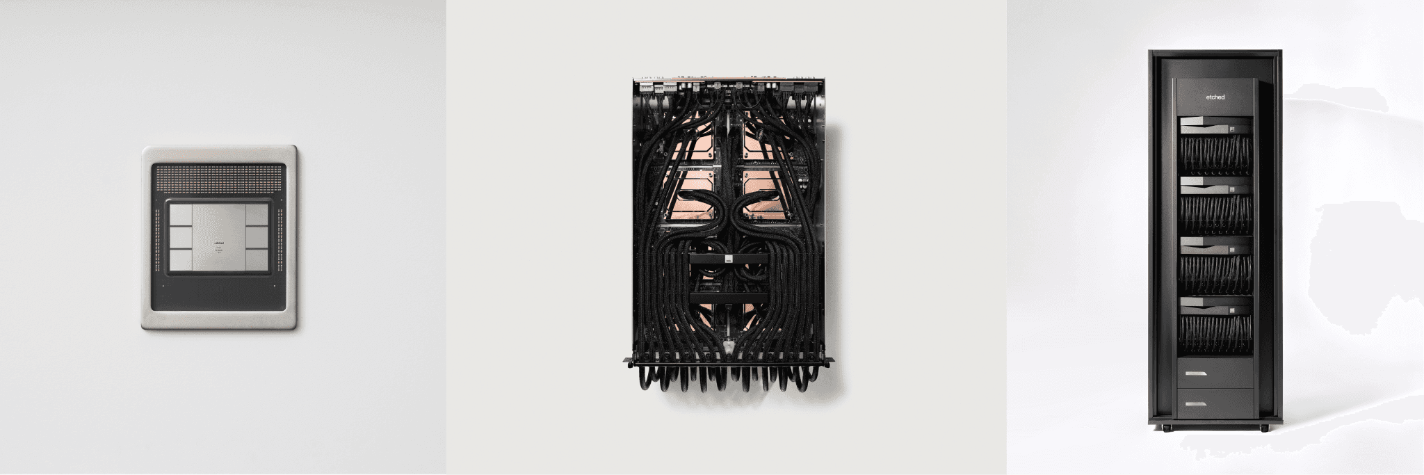
Chip, Rack, Tray by Etched. Image Credit: Etched
5.2.2. d-Matrix: Memory-centric inference
Sid Sheth and Sudeep Bhoja founded d-Matrix in 2019 after observing that inference would eventually require more computing infrastructure than training. The company initially explored analog in-memory computing before shifting to a more scalable digital approach.
Its Corsair platform performs calculations close to SRAM, reducing the time and energy spent moving model data. d-Matrix leads this category because Corsair entered full production in June 2026. It can also complement GPUs by accelerating memory-intensive decode while GPUs handle compute-heavy prefill. The main challenge is customer adoption of a new architecture and software stack.
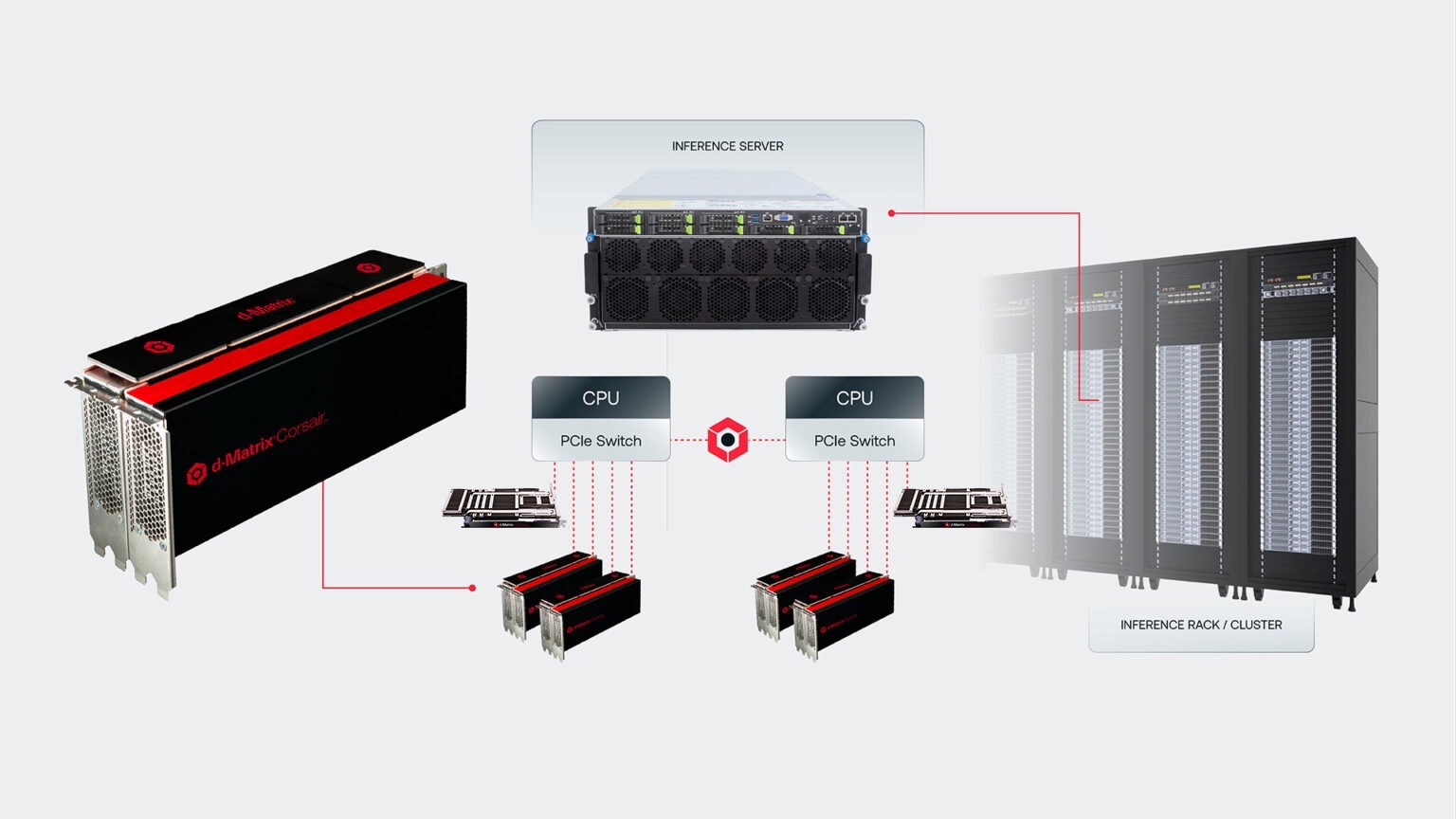
d-Matrix Corsair and Racks. Image Credits: d-Matrix
5.2.3. SambaNova: the mature private full-stack platform
SambaNova was founded in 2017 by Stanford professors Kunle Olukotun and Christopher Ré and former Oracle executive Rodrigo Liang. Their goal was to create an architecture designed around the movement of data through AI models.
Its Reconfigurable Dataflow Unit maps AI models into dataflow graphs rather than conventional instruction sequences. SambaNova combines its chips with systems, software and cloud services. Its fifth-generation SN50 targets large-scale agentic inference, while JPMorganChase’s adoption of SambaNova RDUs provides enterprise validation. The main challenge is the cost of building and operating a complete technology stack.
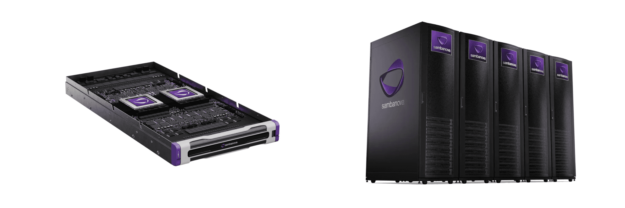
SambaNova RDU Chip and RambaStack. Image Credits: SambaNova
5.2.4. Hailo: the established edge-AI platform
Hailo was founded in Israel in 2017 to bring advanced AI from data centres into cameras, vehicles and industrial devices. Its architecture distributes compute and memory across the chip, enabling vision and generative-AI inference within a small power envelope. Hailo has since released several generations, including Hailo-8, Hailo-10 and Hailo-15.
In July 2026, Microchip Technology (NASDAQ: MCHP) signed a definitive agreement to acquire Hailo for undisclosed terms. The transaction is expected to close by the end of September 2026, subject to regulatory approval and customary conditions. Microchip said Hailo brings more than 100 current customers and a developer community exceeding 10,000 users.
5.2.5. Tenstorrent: Open architecture and licensable IP
Tenstorrent was founded in 2016 by processor engineers Ljubisa Bajic, Ivan Hamer and Milos Trajkovic. It is now led by Jim Keller, whose previous work includes major processor programs at AMD, Apple and Tesla.
Its Tensix cores combine matrix and vector compute, local SRAM and networking, scaling from accelerator cards to Galaxy systems. Tenstorrent can sell chips and systems or license its AI and RISC-V technology to customers developing custom silicon. This gives it several routes to market, although its broader programmability may offer less efficiency than a narrowly optimized ASIC.
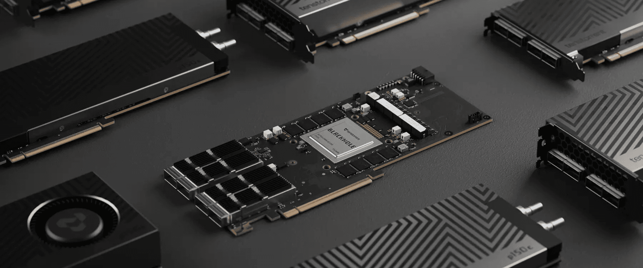
Blackhole with RISC-V cores. Image Credits: Tenstorrent
6. The Chip Is Only the Beginning
A fast ASIC can still become a commercial failure. It may look impressive in a benchmark but struggle when connected to real memory, software and networks or when customers cannot keep it busy. In practice, the winners will need to optimize the entire system, from silicon and packaging to cooling, compilers and cloud deployment.
The hardest trade-off is specialization versus adaptability. Removing unnecessary features can make an ASIC faster and more efficient, but AI models are changing rapidly while manufactured circuits remain fixed. Hyperscalers can spread this risk across enormous internal workloads; merchant-chip companies must persuade outside customers to adopt unfamiliar hardware and software.
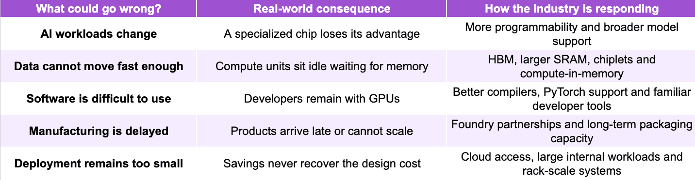
Table 10: Possible challenges and solutions. © 2026 Jarsy Research
The industry may not converge on a single chip that replaces the GPU. Instead, different processors could serve different workloads: GPUs providing flexibility for model development and training, and ASICs handling stable, high-volume inference or specialized edge applications.
An AI travel assistant illustrates how this could work. A low-power chip in a phone or wearable device might process voice and visual inputs, while cloud accelerators handle reasoning and rank flight and hotel options. The underlying models could still be trained on large GPU or TPU clusters. What appears to the user as one service may rely on several types of processors working together.
Further Reading: